
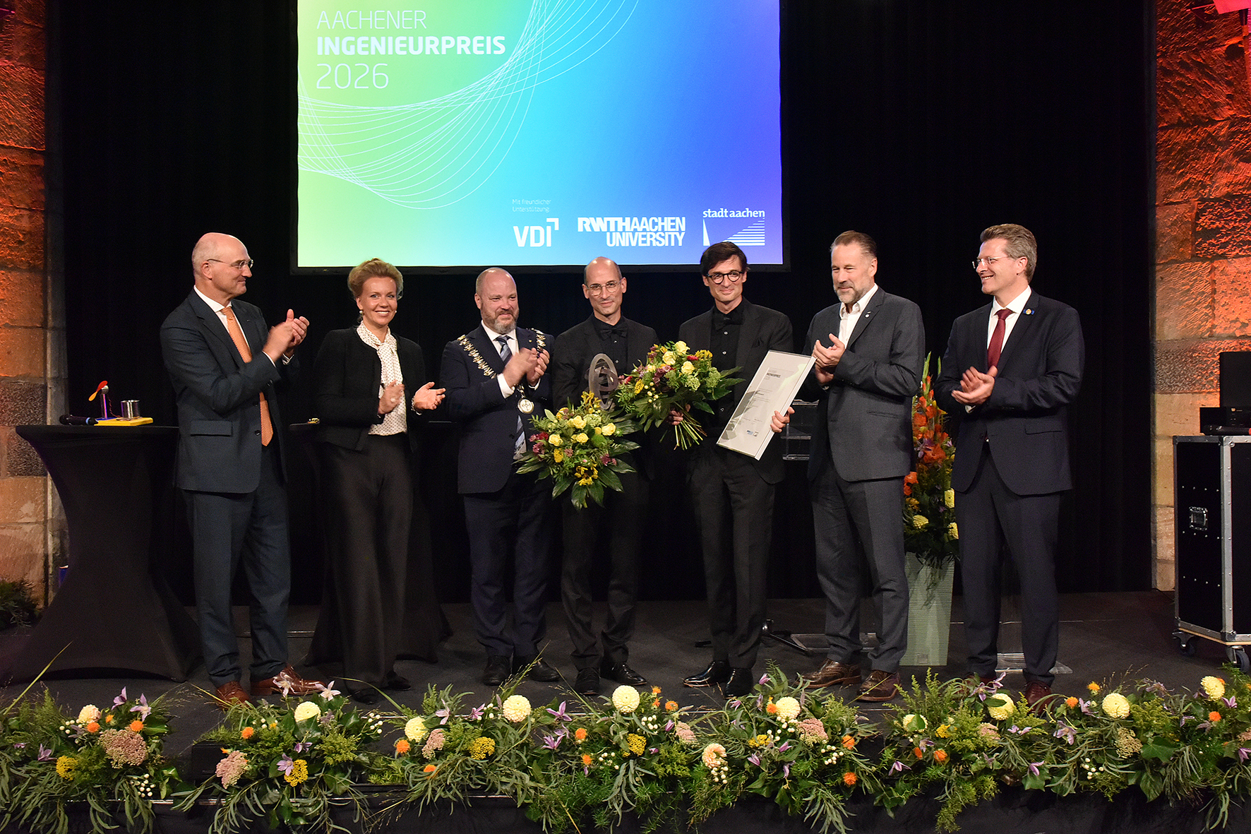
Applause for the award recipients: RWTH President Professor Ulrich Rüdiger, Minister Ina Brandes, Mayor Dr. Michael Ziemons, Sebastian Schall, Dr. Daniel Schall, Professor Max Lemme, and vdi President Professor Lutz Eckstein (from left) © Andreas Herrmann
Daniel and Sebastian Schall were awarded this year’s Aachen Engineering Award for their research on integrated graphene photonics and the founding of their startup, Black Semiconductor. The story of the two brothers illustrates how closely science and entrepreneurship are intertwined in Aachen.
On September 5, 2026, Aachen City Hall’s historic Coronation Hall was transformed into a stage for the future of global microelectronics. The prestigious Aachen Engineering Award was presented for the twelfth time—but with a twist: for the first time ever, the award went to two people. Daniel and Sebastian Schall, the founders of Black Semiconductor, accepted the award together. In doing so, they demonstrated that technological leaps always require two sides of the same coin. While Daniel embodies technological ingenuity as a scientific visionary, Sebastian contributes the drive necessary to transform a complex laboratory idea into a scalable company.
What the award-winning team does not reveal about their areas of responsibility is summed up by the laudatory speaker, Professor Max Lemme, head of the Chair of Electronic Devices at RWTH Aachen University and managing director of AMO GmbH:
“They are fundamentally grounded; they haven’t lost their sense of what truly makes us human.”
Building on this solid foundation, they are looking ahead and developing solutions to problems that conventional systems cannot solve: While the demands placed on systems by data-intensive software architectures and AI models are constantly increasing, the scalability of conventional semiconductor hardware is approaching its physical limits. Guided by the motto “More than Moore,” the Schall brothers are banking on a paradigm shift in the semiconductor industry that seeks to overcome this technological bottleneck: moving away from mere geometric miniaturization toward functional diversification. Instead of forcing performance gains solely through circuit density, new technologies and complementary materials are being integrated directly into the chip.
As a key technology, integrated photonics is already a reality today. The processor performs calculations electrically, as usual. Data transmission, however, takes place via laser through integrated optical waveguides, at the speed of light. This architecture completely eliminates electrical resistance along the communication paths. While, in the current “island solution,” data must travel a few fractions of a millimeter as an electrical current from the main electrical processor to the neighboring photonic chip—where it is converted into light signals—this “bridge” is traversed vertically in a 3D chip architecture: Here, state-of-the-art packaging techniques are used to utilize space in three dimensions, thereby minimizing the path between electrical computing chips and photonic components as much as possible.
Black Semiconductor has now succeeded in achieving direct optical signal conversion at the chip level. Graphene, a two-dimensional carbon lattice, plays a key role in this process. Due to its extreme physical properties, the material is considered a key component for future semiconductor architectures. Because of its single-layer, hexagonal atomic structure, electrons move through it with virtually no resistance, giving graphene extremely high charge carrier mobility. It also offers excellent thermal conductivity and broadband optical absorption. However, in practice, its large-scale application has so far been hindered by a major obstacle: the atomically thin material could not be integrated into industrial manufacturing processes in a defect-free and reproducible manner.
The start-up from Aachen is now bridging this very technological gap, thereby enabling true, monolithic integration of photonics. The graphene structures are deposited directly onto the existing wafer as part of the standard CMOS manufacturing process. By acting as an interface, they enable logical computations and signal conversion on a single physical chip. The startup’s stated goal is to couple thousands of semiconductors so that they function as a single component.
In previous approaches to integrated photonics, data signals must leave the electronic logic layer and travel to the photonic chiplet via physical, metallic interfaces or vertical microcolumns. Although these paths are short, significant losses occur at the metallic interfaces. These error-prone connections, as well as the need for subsequent mechanical assembly steps during manufacturing, will no longer be necessary in the future.
“Their solution is nothing short of a revolution,” said Professor Max Lemme at the Aachen Engineering Award ceremony. “Semiconductors are the brain of AI—a strategic technology, not just a nice-to-have.”
The fact that this development originated in Aachen rather than in Silicon Valley underscores the close link between scientific excellence and application-oriented entrepreneurship within the RWTH Aachen University community. The technological foundation for the spin-off was developed in the laboratories of the research institute AMO GmbH, which is closely integrated with our Faculty of Electrical Engineering and Information Technology and is headed by Professor Max Lemme. While working on his doctoral dissertation, Dr. Daniel Schall found here the specialized cleanroom infrastructure and the scientific freedom he needed to experimentally validate the fundamentals of integrated graphene photonics. The Aachen ecosystem serves as a fertile ground in which excellent basic research and its translation into marketable business structures go hand in hand:
“We always had plans to start the company. Once we knew enough about both physics and technology and could assume that the outstanding challenges in mass production with state-of-the-art equipment could be solved, we simply took the decisive step from the lab to production.”
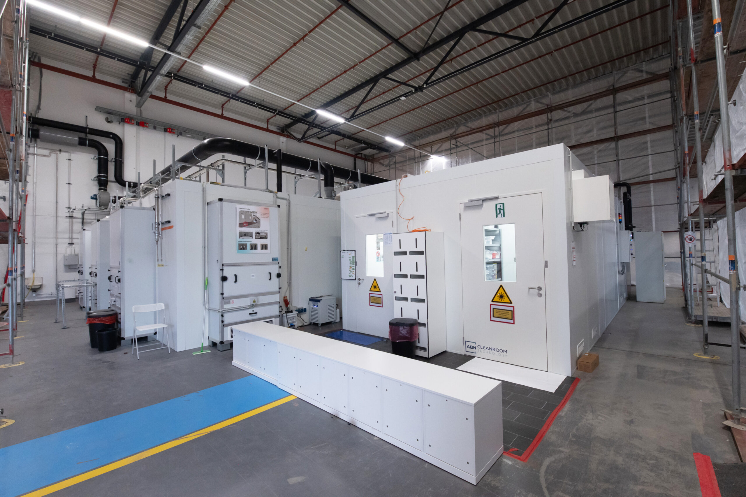
Modular cleanroom facility inside the new FabONE production hall in Aachen-Rothe Erde © Heike Lachmann
This strategic choice of location paves the way for the company’s ambitious growth: With grants and investments totaling over 254 million euros, the startup is driving its expansion forward at a rapid pace. The 15,000-square-meter “FabONE” production facility in Aachen’s Rothe Erde district now employs around 167 international specialists. Their clear goal is to transition innovative graphene chip manufacturing from the laboratory to industrial mass production. Beyond its regional success, this project holds significant geopolitical relevance. At a time when global semiconductor supply chains are subject to technological and political interdependencies, establishing such a key technology in Germany—and thus in the European Union—secures a measure of technological sovereignty.
“Black Semiconductor is sustainably strengthening Europe’s position as a hub for the semiconductor industry, through its close collaboration with research institutions and its industrial focus. The company thus embodies, in a unique way, innovation-driven engineering excellence that is of strategic importance for future technologies,” explains RWTH Rector Professor Ulrich Rüdiger.
It is precisely this combination of pioneering engineering work and strategic significance that forms the basis for the award. The Aachen Engineering Award, which has been presented jointly by RWTH Aachen University and the City of Aachen since 2014, honors individuals who have had a lasting impact on the field of engineering. The award sculpture, “Intersecting Ellipses,” is donated by the Association of German Engineers (VDI) as a key partner of the award. With this win, the Schall brothers join the ranks of renowned award recipients, such as Nobel laureate Emmanuelle Charpentier and technology pioneer Sebastian Thrun, while also sending a clear signal about the innovative strength of Aachen’s electrical engineering community.
The breakthrough in graphene photonics in Aachen is just the beginning of a much larger development: To achieve strategic technological autonomy, the European Union is also investing in graphene and other two-dimensional materials in many other key industries.


Leave a Reply