Kategorie: ‘Mikro- und Nanoeletronik’
How to report and benchmark emerging field-effect transistors
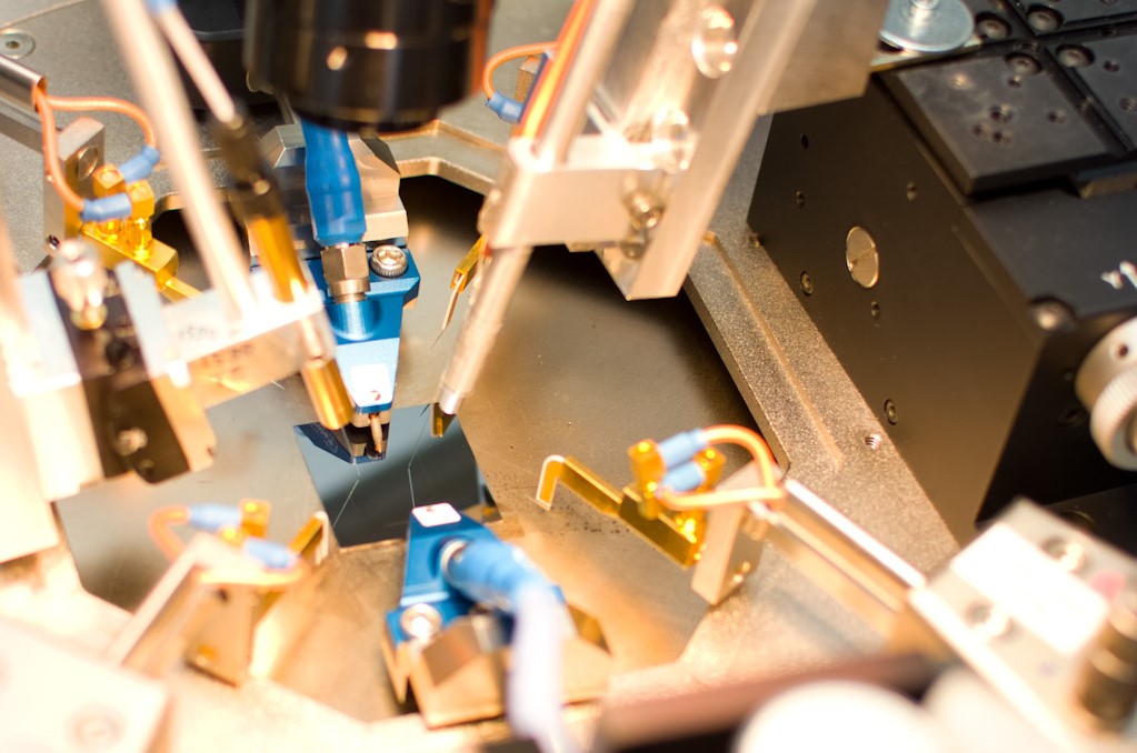
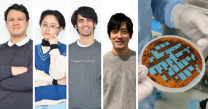
Messungen an einem Graphen-basierten FET in einer Messstation bei AMO. Photo: ©AMO GmbH
One of the challenges encountered by research on novel electronic devices is to compare devices based on different materials in a consistent way. RWTH Professor Max Lemme and colleagues from USA, China, and Belgium have now proposed a set of clear guidelines for benchmarking key parameters and performance metrics of emergent field-effect transistors. The guidelines have been published as a Perspective Article in Nature Electronics.
Research on field-effect transistors (FET) has long explored the possibility of replacing silicon as channel material with emerging nanomaterials, such as carbon nanotubes, graphene, transition metal dichalcogenides, organic semiconductors, or ultrathin oxides. The field is thriving and keeps uncovering fundamental aspects of these materials. But when it comes to comparing the performance of different devices, there is often a lack of consistent reporting and benchmarking
“Assessing consistently the potential of new materials for novel transistors is difficult, because the performance depends on many aspects and details of the device structure, and many parameters are interdependent.” explains Prof. Lemme. Further complexity is added to the field by the interdisciplinarity of the research community, which includes electrical engineers, chemists, materials scientist and physicists. The multitude of approaches increases the challenge of reporting and benchmarking results consistently.
To address this situation, Lemme and colleagues have prepared a checklist of device parameters to be reported, as well as a list of recommended benchmarking plots to compare device parameters and performance metrics. In addition, they present an explicit example of how to use the proposed procedure by applying it to the case of FETs based on monolayer molybdenum disulfide (MoS2), which is one of the emerging materials most studied in recent years for transistor application.
“To identify the real advantages and opportunities offered by novel materials in the search for improved transistors, we need to be able to benchmark and report different devices in a consistent way. We also need to make sure that all relevant data are reported every time.” adds Lemme. “We hope that our work will contribute to bring clarity in the community and guide the search for even better devices.”
Bibliographic info
“How to report and benchmark emerging field-effect transistors”
Z. Cheng, C.-S. Pang, P. Wang, S. T. Le, Y. Wu, D. Shahrjerdi, I. Radu, M. C. Lemme, L.-M. Peng, X. Duan, Z. Chen, J. Appenzeller, S. J. Koester, E. Pop, A. D. Franklin, and C. A. Richter, Nature Electronics 5, 416–423 (2022).
DOI: https://doi.org/10.1038/s41928-022-00798-8
Contact:
AMO GmbH, Gesellschaft für Angewandte Mikro- und Optoelektronik
Otto-Blumenthal-Str.25S
52074 Aachen
haupt@amo.de
Professor Franscesca Santoro received the Leopoldina Early Career Award
 Professor Franscesca Santoro received the Early Career Award from the Leopoldina – National Academy of Sciences on September 23, 2022. She received the €30,000 prize for her research work in the field of bioelectronics and the development of novel materials that can interact with the skin and the brain. You can read more information on the Leopoldina news page.
RWTH student team AixSense successful in international SensUs competition
The Faculty of Electrical Engineering and Information Technology warmly congratulates students Daniyar Kizatov, Jiayi He, Anshul Prashar and Shunjiro Sodei and all involved on their successful second place in the international Biosensor Competition SensUs! The fourth generation of the RWTH Aachen student team AixSense participated in the SensUs competition at Eindhoven University of Technology this year.
Consisting of four ambitious students from the fields of Computer Engineering and Micro-Nano-Electronics, the interdisciplinary team has spent the past six months developing a prototype biosensor to detect the influenza A virus. Thus, the team worked in the laboratories and clean rooms of our Institute of Materials in Electrical Engineering 1 at RWTH, where the chips (see picture on the right) were produced as key components for the technology. The team was supervised by Prof. Sven Ingebrandt and Dr. Vivek Pachauri.
Daniyar Kizatov, Jiayi He, Anshul Prashar, Shunjiro Sodei | Copyright: IWE1
At the final event, the AixSense team presented the biosensor prototype and was awarded in four categories for analytical performance, creativity, transferability of the concept and public inspiration. In the Analytical Performance category, RWTH Aachen University took second place by a slight margin.
“Our team was never so close to winning one of the most important awards. It was very close and we are proud of our performance.”
– Daniyar Kizatov, team leader of AixSense
This year, 14 student teams from Denmark, Egypt, the Netherlands, Germany, Portugal, Switzerland, China, Sweden, the USA, Belgium, the UK, Canada and Spain took part in the competition.
The biosensor has been known to the public at the latest since the introduction of the Covid rapid test – but the SensUs community has been supporting young scientists to present their research in the field of biosensors internationally for five years. Every year, a new generation of teams faces the challenge of developing a biosensor prototype for a new disease. So far, the focus has been on detecting biomarkers for kidney failure, heart failure, antibiotic resistance, rheumatism and epilepsy.
Next year, the SensUs competition aims to detect cytokines as crucial proteins in the immune system. The application phase for the next generation of the AixSense team starts in December 2021 – more information on how to apply can be found here.
(Original article press release IWE1)
(Deutsch) 2Exciting Ausbildungsnetzwerk – Die nächste Generation von 2D-Expert*innen fördern
(Deutsch) Mobilfunkexpertise in Nordrhein-Westfalen – BMBF wählt 6G-Forschungs-Hubs aus
Competence Cluster Battery Utilization Concepts (BattUtilization)
Copyright: ISEA
With the further spread of renewable energies and electromobility, powerful and reliable energy storage systems are becoming increasingly important. When is the secondary use of battery storage possible and for which applications is it useful? This question is being addressed by the project partners from research and industry in the new Battery Utilization Concepts ( BattNutzung) cluster, which is being funded by the German Federal Ministry of Education and Research with around 20 million euros. The cluster is coordinated by Prof. Sauer from ISEA. Together with the competence cluster greenBatt, the BattNutzung cluster forms the cross-sectional initiative “Battery Life Cycle”. This aims at a holistic view of second use and recycling concepts, which is to be enabled by linking the two clusters and through a cross-cluster exchange.
Future cluster NeuroSys – Interview with Professor Lemme

The future cluster initiative “Clusters4Future” of the Federal Ministry of Education and Research promotes innovations that go hand in hand with the growing needs of our society. One of the winners of this ideas competition is the cluster “NeuroSys – Neuromorphic Hardware for Autonomous Artificial Intelligence Systems”, which is coordinated by Prof. Dr. -Ing. Max Christian Lemme from the Chair of Electronic Components. The future cluster “NeuroSys” researches adaptive and energy-efficient hardware that is oriented towards the way the brain works. The goal behind this is to allow intelligent and resource-saving on-site data processing and thus create an essential prerequisite for AI applications.
Watch the interview on this page or directly on our YouTube Channel
How catalysts become more active
Researchers from Jülich, Aachen, Stanford, and Berkeley have studied the layer-by-layer structure of catalyst material. They have discovered that a surface layer as thin as a single atom can double the activity for the reaction of water splitting – without increasing the energy consumption. This also doubles the amount of hydrogen produced.
The scientists hope that this increased understanding will allow developing better catalysts in the future to produce green hydrogen more energy-efficiently, and thus more cost-effectively, than before. Hydrogen is called green when it is produced by the electrolysis of water in a climate-neutral way using electricity from renewable sources. Hydrogen is regarded as an essential building block of the energy transition, partly because it can store wind and solar energy in times of oversupply and release it again later.
Part of the research results came about at the Peter Gruenberg Institute, Electronic Materials Division, in the Electronic Oxide Cluster Laboratory of Professor Regina Dittmann.
Original publication: ‘Tuning electrochemically driven surface transformation in atomically flat LaNiO3 thin films for enhanced water electrolysis’
C. Baeumer, J. Li, Q. Lu, A. Liang, L. Jin, H. Martins, T. Duchoň, M. Glöß, S. M. Gericke, M. A. Wohlgemuth, M. Giesen, E. E. Penn, R. Dittmann, F. Gunkel, R. Waser, M. Bajdich, S. Nemšák, J. T. Mefford, W. C. Chueh
Nature Materials, 11 January 2021, DOI: 10.1038/s41563-020-00877-1
Find further information on the website of the Jülich Research Centeer
Publication – Contactless, Battery-free, and Stretchable Wearable for Continuous Recording of Seismocardiograms
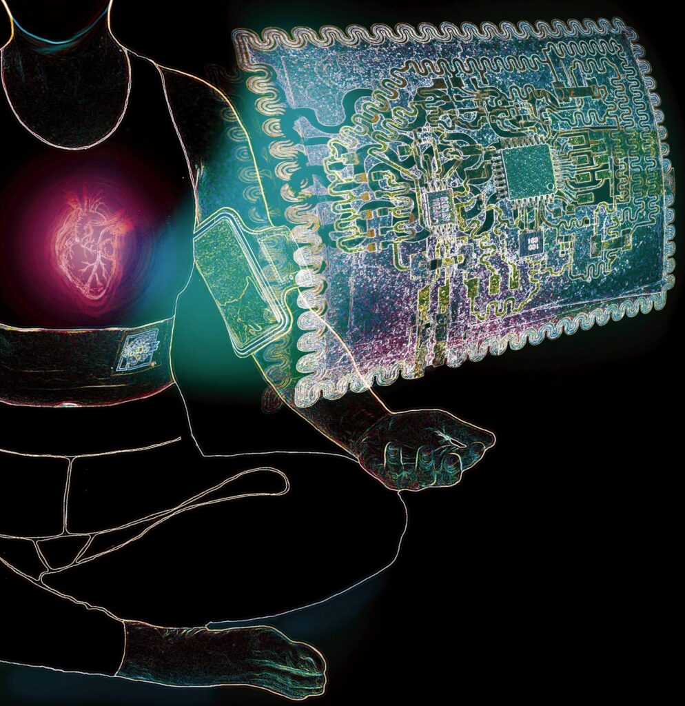
Photo: IWE1
Prof. Dr.rer.nat. Sven Ingebrandt and his research team published the article “Contactless, Battery-free, and Stretchable Wearable for Continuous Recording of Seismocardiograms” in the journal ACS Applied Electronic Materials.. This article presents a study to enable remote measurement of mechanical cardiac activity using a contactless wearable patch and seismocardiography (SCG). Near-field communication (NFC) technology is used for power supply and wireless recording of SCG data. A separate electrocardiogram (ECG) is used as a reference. The results of this study show a good signal-to-noise ratio and a close correlation between SCG and ECG recordings. This method could become another valuable tool for cardiac monitoring in the future.
Contactless, Battery-free, and Stretchable Wearable for Continuous Recording of Seismocardiograms
2D materials for high-volume production of electronic components
RWTH Professor Max Lemme and research partners publish in Journal “Nature Communications”
Professor Max Lemme, Chair of Electronic Devices at RWTH Aachen University, and his research partners publish a new method to integrate 2D materials into semiconductor manufacturing lines in the journal Nature Communications. The RWTH Aachen University researchers were supported by the KTH Royal Institute of Technology in Stockholm, the University of the Federal Armed Forces in Munich, AMO GmbH and Protemics GmbH. Currently, most experimental methods are not compatible with large-scale production. Moreover, they lead to significant degradation of the 2D material and its electronic properties. The method now being researched attempts to solve these problems. The two-dimensional materials will enable devices with significantly smaller sizes and enhanced functionalities compared to current silicon technologies. Overall, the range of potential applications extends from photonics to sensor technology and neuromorphic computing.
Further information on the website of AMO GmbH

