
Schlagwort: ‘Lehrstuhls für Elektronische Bauelemente’
New dimensions for microelectronics: RWTH and TU Dresden launch major joint project

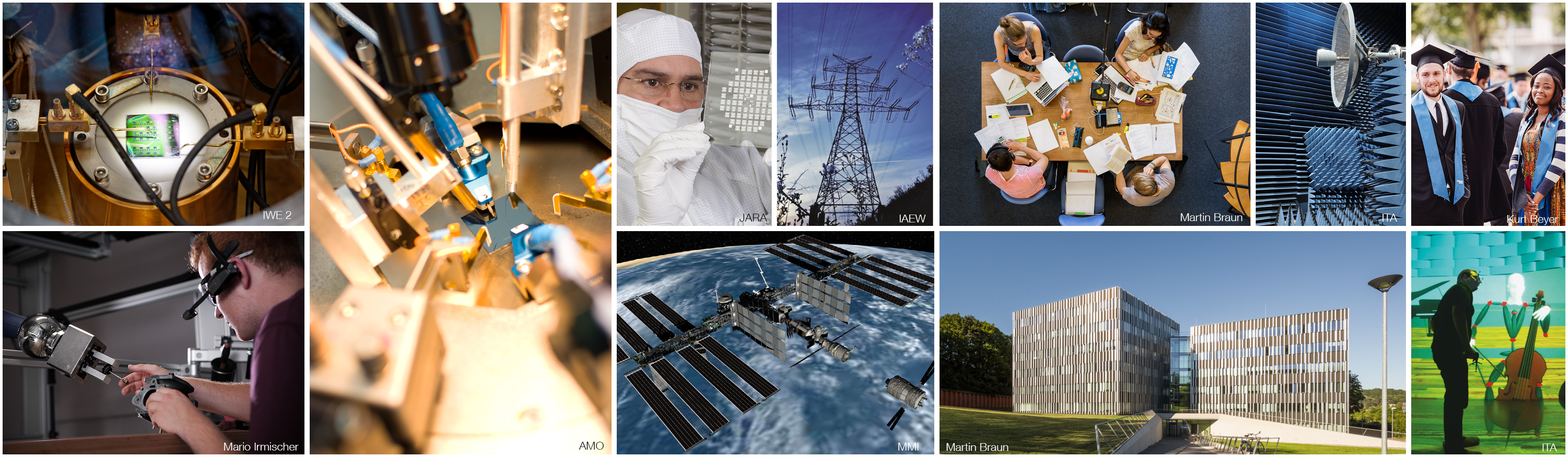
Artistic visualization of a stacked chip resembling a skyscraper. © TU Dresden / cfaed
Professor Max Lemme is the co-spokesperson for the new DFG Collaborative Research Centre, ‘Active-3D’. The project aims to enhance the performance of microchips by utilising the previously unused space above the chip surface.
The Deutsche Forschungsgemeinschaft (DFG, German Research Foundation) is establishing a new Collaborative Research Centres/Transregios (CRC/TRR-404), namly Next Generation Electronics with Active Devices in Three Dimensions (Active-3D). This pioneering research project aims to take the miniaturisation of microelectronics to the next phase. With Professor Max Lemme, holder of the Chair of Electronic Devices at RWTH Aachen University, a renowned scientist from the Faculty of Electrical Engineering and Information Technology is involved in a central role as co-spokesperson. Together with Professor Thomas Mikolajick from TU Dresden, he is coordinating the joint project, in which several universities and non-university research institutions are involved.
The aim of the Collaborative Research Centre is to make the third dimension electronically usable. While conventional chips have mainly been optimised in terms of surface area, the volume above this – i.e. the area of the so-called metallisation level (back-end of line, BEOL) – is now also to be developed for active components that enable logic and memory functions as well as switchable connections. Based on new materials, innovative components are being developed and integrated into circuits and systems that offer enhanced performance, processing speed and surface area. As part of the technology-design-system co-development approach, materials, technology and circuits are being developed simultaneously. This makes it possible to distribute functionalities across the volume previously reserved for passive wiring, thus utilising the entire volume of the chip. The result could be completely new 3D electronic systems that are not only more powerful, but also more energy-efficient and compact.
‘The TRR Next Generation Electronics With Active Devices in Three Dimensions (Active-3D) will strengthen Germany’s and Europe’s position in basic microelectronics research,’ explains Professor Mikolajick. ‘The researchers involved at the various locations are ideally placed to investigate the use of the entire volume of a chip for active components.’
This major project has already resulted in the formation of a powerful network at the forefront of international electronics research. Partners include Forschungszentrum Jülich, AMO GmbH, NaMLab gGmbH, the Max Planck Institute of Microstructure Physics in Halle, and Ruhr University Bochum. The Collaborative Research Centre/Transregio format enables close, cross-location cooperation. RWTH Aachen University and TU Dresden share scientific responsibility, each contributing complementary focal points. In addition, young scientists from other universities and non-university research institutions are involved. Around 15 doctoral and postdoctoral positions have already been filled, with one further position yet to be advertised. Further vacancies will follow during the course of the project.
Vacancies will be posted on the homepage of the Max Planck Institute of Microstructure Physics.
Graphene in microelectronics – research for series production

Professor Max Lemme holds the Chair of Electronic Devices at RWTH Aachen University and is Director of the non-profit research organisation AMO GmbH. © Martin Braun
As part of the completed European 2D-Experimental Pilot Line (2D-EPL) project, AMO GmbH has realized two multi-project wafer runs for the large-scale production of electronic devices based on graphene.
The discovery of graphene and other two-dimensional materials in 2004 was seen as potentially revolutionary for advances in microelectronics. The material’s high carrier mobility, broadband optical absorption, low thickness and high mechanical strength have raised great expectations for the use of graphene in electronics, optoelectronics and sensor technology.
‘There are now plenty of publications that show prototypes of devices based on 2D materials with performances significantly beyond the state-of-the-art,’ says Cedric Huyghebaert, technical leader of the 2D-EPL project.
However, the semiconductor industry has not yet produced any commercially viable graphene devices. This is due to a number of challenges, including but not limited to graphene growth, graphene transfer and purification. The transition from scientific experiments involving only a small number of graphene devices to real applications based on reliable manufacturing processes for mass production has stagnated.
The 2D-EPL project, which was funded by the European Commission, was a €20 million initiative that sought to demonstrate the technical feasibility of manufacturing devices based on graphene and other two-dimensional materials on a large scale. The primary objective of this project was to promote market feasibility. In pursuit of this objective, all actors involved in the value chain were convened between October 2020 and September 2024, resulting in the execution of five multi-project wafer (MPW) runs. In addition to the development of process modules at an industrial level, the delivery of graphene-based devices to customers was a further objective. Each of these runs provided universities, research institutes and companies with the opportunity to customise their components on a wafer chip.
‘Our final goal is to demonstrate that it is possible to produce a wide range of devices based on two-dimensional materials in a way that is interesting for industry, and each multi-project wafer run wants to set a milestone in that direction,’ explains Professor Max Lemme, scientific director of AMO GmbH and holder of the Chair of Electronic Devices at RWTH Aachen University
AMO GmbH has successfully executed the inaugural and third multi-project wafer run in a cutting-edge clean room facility. The initial MPW run addressed the definition of graphene field-effect transistors with exposed graphene channels, with a focus on their applications in chemical and biosensor technologies. The subsequent MPW run dealt with the definition of transistors with dielectric encapsulation, which were intended for utilisation in electronic applications. The specified device performance parameters for mobility, charge neutral point, sheet resistance and contact resistivity were measured. Should the target values be realised and the optical microscopic analysis demonstrate acceptable quality with regard to lift-off and etching, the wafer would be deemed ready for delivery. The researchers confirmed the existence of challenges that had previously been identified, including the formation of residue from the resist, which can present difficulties in the context of biosensor applications, given the necessity of a pure graphene surface. Furthermore, there were still unknown problems at the time, such as unexpected customer-specific requirements and their technical realisation, which had to be solved.
‘We consider the wafer runs to be successful because the device yield and performance met or exceeded the initial specifications across the wafers. In addition, all customers were served with little or no delay,’ reads the scientific article presenting the results of the first and third multi-project wafer runs.
The results of the five multi-project wafer runs form the basis of the follow-up project 2D-Pilot Line (2D-PL). The objective of the present pilot line is to further strengthen the European ecosystem in the development of integration modules for photonics and electronics prototyping services. The work is centred on the maturation of semiconductor technologies and the provision of information to support industrial deployment. In this context, comprehensive prototyping services are offered for the integration of 2D materials, such as graphene, on established semiconductor platforms with silicon technologies.
The scientific article Multi-project wafer runs for electronic graphene devices in the European 2D-Experimental Pilot Line project provides further insights into the multi-project wafer runs one and three.
Further information on the topic can be found on the homepage of the Chair of Electronic Devices.
The 2023 Annual Report of the Graphene Flagship provides an overview of the work of the 2D Experimental Pilot Line, presenting the current status of 2D materials research in Europe and new projects.


